
India launches first 3D glass semiconductor packaging unit in Odisha
Updated: Apr 20th, 2026
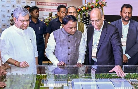 India has launched the first 3D glass based semiconductor packaging unit in Bhubaneswar, Odisha. The project, worth ₹1,943 crore, is being developed by 3D Glass Solutions Inc. This step will help India enter advanced chip technology and reduce dependence on imports.
The unit will use 3D Heterogeneous Integration (3DHI) technology to stack chips, making them faster, more efficient, and energy-saving. It will mainly support sectors like AI, data centers, defense, and future 5G/6G communication.
Unlike traditional silicon, glass improves performance by reducing signal loss and handling high temperatures better. This makes chips more powerful without making them smaller.
The plant aims to produce around 50 million units per year and create over 2,500 jobs. It is part of India’s plan to build a complete semiconductor ecosystem in the country.
Union Minister Ashwini Vaishnaw called it a historic step and said Odisha is becoming a hub for high-tech industries. The government also plans to expand the plant’s capacity in the future.
Commercial production is expected to start by 2028, helping India become a global player in next-generation chip technology and strengthening its position in the global semiconductor race.